Topic: Analog Circuits
The voltage V in the circuit given below is :
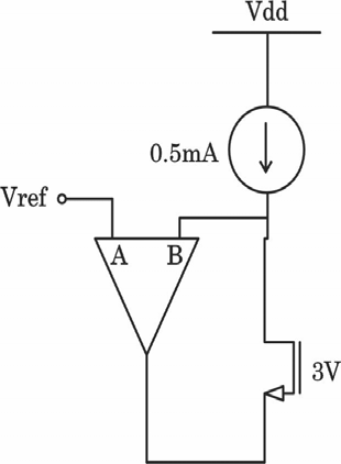
- A. Terminal A is positive. Terminal B is negative
- B. Terminal A is negative. Terminal B is positive
- C. Both of above
- D. None of the above
Answer: B. Terminal A is negative. Terminal B is positive
Explanation: 1. **Feedback Polarity:** The OPAMP drives the gate of the NMOS transistor. The drain of the NMOS is connected to terminal B. If the voltage at B increases, the OPAMP output should increase the gate voltage to turn the NMOS ON harder, pulling the drain voltage (B) back down. This requires terminal B to be the non-inverting (+) terminal. Therefore, terminal A must be the inverting (-) terminal.
2. **Gate Potential:** By virtual short, $V_B = V_{ref} = 3V$. The transistor is in saturation since it's driven by a 0.5mA current source. $I_D = \frac{1}{2} \mu_n C_{ox} (\frac{W}{L}) (V_{GS} - V_T)^2$. Substituting the values: $0.5 = \frac{1}{2} (1) (V_G - 3 - 0.7)^2$. Solving this: $1 = (V_G - 3.7)^2 \implies V_G = 3.7 + 1 = 4.7V$.