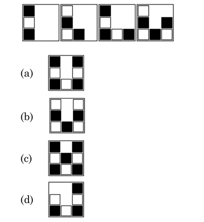
ISRO Electronics & Communication (ECE) 2025 Question Paper & Solutions
Attempt the ISRO Electronics & Communication (ECE) 2025 previous year paper in real CBT exam mode or practice mode with verified answers and explanations.
All ISRO Electronics & Communication (ECE) papers
95 questions. Answers are shown only where the official answer key is available.
Question 1
Topic: Signals and Systems
For the following function, poles and zeros will be:
$x(t)=\delta(t)-\frac{4}{3}e^{-t}u(t)+\frac{1}{3}e^{2t}u(t)$
- A. Poles at -1 and 2, Zero at -1
- B. Poles at -1 and 2, Zero at 1
- C. Poles at -1 and -2, Zero at -1
- D. Poles at 1 and -2, Zero at -1
Answer: B. Poles at -1 and 2, Zero at 1
Explanation: Taking the Laplace transform of the given function:
$X(s) = 1 - \frac{4/3}{s+1} + \frac{1/3}{s-2}$
$X(s) = \frac{3(s+1)(s-2) - 4(s-2) + (s+1)}{3(s+1)(s-2)}$
$X(s) = \frac{3(s^2 - s - 2) - 4s + 8 + s + 1}{3(s+1)(s-2)}$
$X(s) = \frac{3s^2 - 3s - 6 - 3s + 9}{3(s+1)(s-2)} = \frac{3s^2 - 6s + 3}{3(s+1)(s-2)} = \frac{3(s-1)^2}{3(s+1)(s-2)}$
Simplifying, $X(s) = \frac{(s-1)^2}{(s+1)(s-2)}$.
This gives a double zero at $s = 1$, and poles at $s = -1$ and $s = 2$. Option (b) is the best matching choice.
Question 2
Topic: Analog Circuits / Electromagnetics
A source with internal resistance $Rs=50~\Omega$ is to be matched to a load $RL=200~\Omega$ using a lossless LC network at a frequency of 10 MHz. Which of the following configurations will provide proper impedance matching and high-pass filtering?
- A. A series inductor followed by a parallel capacitor
- B. A parallel inductor followed by a series capacitor
- C. A series capacitor followed by a parallel inductor
- D. A parallel capacitor followed by a series inductor
Answer: C. A series capacitor followed by a parallel inductor
Explanation: To achieve a high-pass filter response, the series element must block low frequencies (so it must be a capacitor) and the shunt (parallel) element must short low frequencies to ground (so it must be an inductor). Since $R_L > R_S$ (200 $\Omega$ > 50 $\Omega$), the standard L-section matching network places the shunt element in parallel with the higher resistance (the load). Therefore, the correct configuration from source to load is a series capacitor followed by a parallel inductor.
Question 3
Topic: Analog Circuits
In Miller's theorem, if a capacitor C is connected between the input and output of an amplifier with gain A, the equivalent input capacitance is :
- A. C
- B. $(1+A)C$
- C. $(1-A)C$
- D. $C/(1+A)$
Answer: C. $(1-A)C$
Explanation: According to Miller's theorem, an impedance $Z$ connected between the input and output nodes of an amplifier with voltage gain $A$ can be represented as an equivalent input impedance $Z_{in} = \frac{Z}{1-A}$. For a capacitor, $Z = \frac{1}{sC}$. Thus, $Z_{in} = \frac{1}{sC(1-A)}$, which corresponds to an equivalent input capacitance of $C_{in} = C(1-A)$.
Question 4
Topic: Signals and Systems
Which of the three signals given below is periodic?
$x_{1}(t)=2e^{j(t+\frac{\pi}{4})}u(t)$
$x_{2}(n)=u[n]+u[-n]$
$x_{3}(t)=\sum_{k=-\infty}^{\infty}\\{\delta[n-4k]-\delta[n-1-4k]\\}$
- A. $x_{1}(t)$
- B. $x_{2}(n)$
- C. $x_{3}(t)$
- D. None of the above
Answer: C. $x_{3}(t)$
Explanation: $x_1(t)$ is multiplied by the step function $u(t)$, meaning it is zero for $t < 0$, so it is not periodic. $x_2(n) = u[n] + u[-n]$ equals 1 for all $n \neq 0$ and 2 for $n=0$ (or 1 depending on step definition), which is a constant with an anomaly at the origin, thus not periodic. $x_3(n)$ (written as $x_3(t)$ in the question but indexed with n) is a summation of shifted impulses that repeats every 4 samples exactly, making it a periodic sequence with period $N=4$.
Question 5
Topic: Electromagnetics / Antennas
A $\lambda/4$ monopole antenna radiates 20 W with gain of 3 dBi. What is its Effective Isotropic Radiated Power?
- A. 10 W
- B. 20 W
- C. 40 W
- D. 60 W
Answer: C. 40 W
Explanation: Effective Isotropic Radiated Power (EIRP) is the product of the transmitted power and the antenna gain expressed in linear scale. Gain in linear scale = $10^{(3/10)} \approx 2$. Therefore, EIRP = $20~W \times 2 = 40~W$.
Question 6
Topic: Analog Circuits
What is a key advantage of Class AB amplifiers over Class B?
- A. Lower bias current
- B. Higher crossover distortion
- C. No need for heat sinks
- D. Reduced crossover distortion
Answer: D. Reduced crossover distortion
Explanation: Class B amplifiers suffer from crossover distortion because the transistors stop conducting when the input signal is near zero volts (within the threshold deadband). Class AB amplifiers solve this by providing a small quiescent bias current to keep the transistors slightly on, thereby significantly reducing crossover distortion.
Question 7
Topic: Signals and Systems
Signal $x[t]=\frac{\sin(100\pi t)}{\pi t}$ is
- A. Time limited and band limited
- B. Time limited but not band limited
- C. Not time limited but band limited
- D. Neither time limited nor band limited
Answer: C. Not time limited but band limited
Explanation: The given signal is a sinc function in the time domain, which extends from $-\infty$ to $+\infty$, making it not time-limited. Its Fourier transform is a rectangular pulse in the frequency domain, strictly confined between $-\omega_c$ and $+\omega_c$ (where $\omega_c = 100\pi$), meaning it is strictly band-limited.
Question 8
Topic: Microwave Engineering
Which device is typically used for low noise amplification in microwave receivers?
- A. Klystron
- B. Travelling Wave Tube Amplifier
- C. Tunnel Diode
- D. HEMT
Answer: D. HEMT
Explanation: High Electron Mobility Transistors (HEMTs) are solid-state devices specifically engineered for high gain and exceptionally low noise figure at microwave and millimeter-wave frequencies. They are widely used as Low Noise Amplifiers (LNAs) in receiver front-ends.
Question 9
Topic: Analog Circuits
Which of the following conditions must hold true for the virtual ground assumption to be valid in an op-amp circuit?
- A. The op-amp must have infinite input impedance and zero output impedance
- B. The op-amp must be operated in open-loop mode
- C. Negative feedback must be present and the op-amp should be operating in the linear region
- D. The op-amp should have a very low gain
Answer: C. Negative feedback must be present and the op-amp should be operating in the linear region
Explanation: The virtual ground concept assumes the voltage difference between the inverting and non-inverting input terminals is zero. This happens because the op-amp has very high open-loop gain; to maintain a finite output voltage (operating in the linear region), the differential input must be virtually zero. This requires negative feedback to stabilize the output and keep it from saturating.
Question 10
Topic: Digital Communications
Given source symbols $A(0.4)$, $B(0.3)$, $C(0.2)$, $D(0.1)$. What is the average codeword length using Huffman coding?
- A. 1.9 bits
- B. 2.0 bits
- C. 2.2 bits
- D. 1.8 bits
Answer: A. 1.9 bits
Explanation: Following the Huffman coding procedure:
1. Combine C(0.2) and D(0.1) -> Node CD(0.3).
2. Combine B(0.3) and CD(0.3) -> Node BCD(0.6).
3. Combine A(0.4) and BCD(0.6) -> Root(1.0).
Tracing back, the lengths are: A = 1 bit, B = 2 bits, C = 3 bits, D = 3 bits.
Average length $L_{avg} = (0.4 \times 1) + (0.3 \times 2) + (0.2 \times 3) + (0.1 \times 3) = 0.4 + 0.6 + 0.6 + 0.3 = 1.9$ bits.
Question 11
Topic: Electromagnetics
A lossless transmission line is 80 cm long and operates at a frequency of 600 MHz. The line parameters are $L=0.25~\mu H/m$ and $C=100~pF/m$. Find the phase velocity:
- A. $3\times10^{8}m/s$
- B. $2\times10^{8}m/s$
- C. $4\times10^{8}m/s$
- D. $6\times10^{8}m/s$
Answer: B. $2\times10^{8}m/s$
Explanation: The phase velocity $v_p$ of a lossless transmission line is given by $v_p = \frac{1}{\sqrt{LC}}$.
$v_p = \frac{1}{\sqrt{(0.25 \times 10^{-6}) \times (100 \times 10^{-12})}}$
$v_p = \frac{1}{\sqrt{25 \times 10^{-18}}} = \frac{1}{5 \times 10^{-9}} = 0.2 \times 10^9 = 2 \times 10^8~m/s$.
Question 12
Topic: Digital Logic / VHDL
In VHDL simulation, consider the following process:
```vhdl
signal A, B: std_logic :='0';
process
begin
A<='1';
B<=A;
wait;
end process;
```
What will be the value of signal B immediately after simulation starts?
- A. '1'
- B. '0'
- C. 'U' (undefined)
- D. Z
Answer: B. '0'
Explanation: In VHDL, signal assignments using `<=` inside a process are not updated immediately; they are scheduled to be updated at the end of the current simulation delta cycle. When `B<=A;` evaluates, signal `A` has not yet changed to '1' and still holds its initial value '0'. Thus, B gets assigned '0', and the process then suspends at the `wait;` statement.
Question 13
Topic: Signals and Systems
Inverse of Laplace transform of $\frac{10}{s^{2}+5s+4}$ is
- A. $10[e^{-t}+e^{-4t}]$
- B. $10[e^{-t}-e^{-4t}]$
- C. $\frac{10}{3}[e^{-t}+e^{-4t}]$
- D. $\frac{10}{3}[e^{-t}-e^{-4t}]$
Answer: D. $\frac{10}{3}[e^{-t}-e^{-4t}]$
Explanation: Factor the denominator: $s^2 + 5s + 4 = (s+1)(s+4)$.
Perform partial fraction decomposition: $\frac{10}{(s+1)(s+4)} = \frac{A}{s+1} + \frac{B}{s+4}$.
$A = \left. \frac{10}{s+4} \right|_{s=-1} = \frac{10}{3}$
$B = \left. \frac{10}{s+1} \right|_{s=-4} = \frac{10}{-3} = -\frac{10}{3}$
$F(s) = \frac{10/3}{s+1} - \frac{10/3}{s+4}$.
Taking the inverse Laplace transform: $f(t) = \frac{10}{3}[e^{-t} - e^{-4t}]u(t)$.
Question 14
Topic: Digital Communications
Which performance metric is minimized in the Minimum Mean Square Error (MMSE) equalizer?
- A. Bit error rate
- B. Mean squared error between transmitted and received signals
- C. Inter-symbol interference
- D. Noise power
Answer: B. Mean squared error between transmitted and received signals
Explanation: An MMSE equalizer is designed to minimize the expected mean squared error between the actual transmitted symbol and the equalizer's output estimate (derived from the received signal). It provides a balance between removing Inter-Symbol Interference (ISI) and preventing excessive noise enhancement.
Question 15
Topic: Control Systems / Power Electronics
Which statement best describes the practical utility of Middlebrook's Theorem?
- A. It replaces needs all for simulation
- B. It allows simplification of component count in circuits
- C. It predicts stability in cascaded systems based on impedance interaction
- D. It eliminates switching losses in converters
Answer: C. It predicts stability in cascaded systems based on impedance interaction
Explanation: Middlebrook's Extra Element Theorem (and the related impedance criterion) is widely used in power electronics to analyze and predict the stability of cascaded subsystems (such as an input EMI filter cascaded with a switching DC-DC converter). It determines stability by assessing the interaction between the output impedance of the source and the input impedance of the load.
Question 16
Topic: Analog Communications
A 10 kW carrier is sinusoidally modulated by two carriers corresponding to amplitude modulation index of 30% and 40% respectively. The total radiated power is
- A. 11.25 kW
- B. 10 kW
- C. 20 kW
- D. 5 kW
Answer: A. 11.25 kW
Explanation: For multi-tone Amplitude Modulation, the total effective modulation index is $m_t = \sqrt{m_1^2 + m_2^2} = \sqrt{0.3^2 + 0.4^2} = \sqrt{0.09 + 0.16} = \sqrt{0.25} = 0.5$.
The total radiated power is $P_t = P_c \left(1 + \frac{m_t^2}{2}\right)$.
$P_t = 10 \left(1 + \frac{0.5^2}{2}\right) = 10 \left(1 + \frac{0.25}{2}\right) = 10 (1 + 0.125) = 11.25$ kW.
Question 17
Topic: Signals and Systems
The Z-transform of a signal $x[n]=\delta[n-k]$, (where k is a positive integer) is:
- A. $z^{k}$
- B. $z^{-k}$
- C. 1
- D. $\delta[z]$
Answer: B. $z^{-k}$
Explanation: By definition, the Z-transform of a discrete-time signal $x[n]$ is $X(z) = \sum_{n=-\infty}^{\infty} x[n] z^{-n}$.
For $x[n] = \delta[n-k]$, the signal is 1 only when $n = k$ and 0 otherwise.
Therefore, $X(z) = \sum_{n=-\infty}^{\infty} \delta[n-k] z^{-n} = 1 \cdot z^{-k} = z^{-k}$.
Question 18
Topic: Probability and Stochastic Processes
Which distribution is memoryless?
- A. Normal
- B. Log-normal
- C. Exponential
- D. None of the above
Answer: C. Exponential
Explanation: The exponential distribution is the only continuous probability distribution that possesses the memoryless property. Mathematically, it satisfies $P(X > s + t | X > s) = P(X > t)$ for all $s, t > 0$. In the discrete domain, the geometric distribution is the only one with this property.
Question 19
Topic: Electromagnetics / Transmission Lines
A one wavelength long, 50 ohm line is terminated in $Z_L=30-j40$ ohms. Its input terminals are connected to the load end of a 100 ohm, quarter-wavelength line. What is the impedance seen at the input to the 100 ohm line?
- A. $30+j40$
- B. $60+j40$
- C. $120+j160$
- D. None of the above
Answer: C. $120+j160$
Explanation: A transmission line of length $n\lambda$ (where $n$ is an integer) repeats the load impedance at its input. Thus, for the $1\lambda$ long $50~\Omega$ line, its input impedance is $Z_{in1} = Z_L = 30-j40~\Omega$.
This $Z_{in1}$ acts as the load for the subsequent $\lambda/4$ line ($Z_{02} = 100~\Omega$).
For a quarter-wavelength line, the input impedance is $Z_{in} = \frac{Z_0^2}{Z_{load}} = \frac{100^2}{30-j40}$.
$Z_{in} = \frac{10000}{30-j40} = \frac{10000(30+j40)}{(30-j40)(30+j40)} = \frac{10000(30+j40)}{30^2+40^2} = \frac{10000(30+j40)}{2500} = 4(30+j40) = 120+j160~\Omega$.
Question 20
Topic: Signals and Systems
A discrete-time LTI system has impulse response $h[n]=\delta[n]+\delta[n-1]$. What is its output $y[n]$ for an input $x[n]=u[n]$?
- A. $u[n]+u[n-1]$
- B. $2u[n]$
- C. $\delta[n]+\delta[n-1]$
- D. $u[n]$
Answer: A. $u[n]+u[n-1]$
Explanation: The output of an LTI system is the convolution of its input and impulse response: $y[n] = x[n] * h[n]$.
$y[n] = x[n] * (\delta[n] + \delta[n-1])$
By the shifting property of the delta function, $x[n] * \delta[n-k] = x[n-k]$.
$y[n] = x[n] + x[n-1]$. Since $x[n] = u[n]$, we have $y[n] = u[n] + u[n-1]$.
Question 21
Topic: Probability and Stochastic Processes
Customer arrivals at a bank follow a Poisson process with mean 10 per hour. What is the probability that time between two arrivals is greater than 10 minutes?
- A. $\exp(-10/6)\approx0.188$
- B. $\exp(-1)\approx0.368$
- C. $\exp(-5/6)\approx0.435$
- D. $1-\exp(-5/6)\approx0.565$
Answer: A. $\exp(-10/6)\approx0.188$
Explanation: For a Poisson process, the time between arrivals (inter-arrival time $T$) follows an exponential distribution with parameter $\lambda$.
Given arrival rate $\lambda = 10$ arrivals/hour. Converting to minutes, $\lambda = 10/60 = 1/6$ arrivals/minute.
The probability that the inter-arrival time is greater than $t$ minutes is $P(T > t) = e^{-\lambda t}$.
For $t = 10$ minutes, $P(T > 10) = e^{-(1/6) \times 10} = e^{-10/6}$.
$e^{-1.667} \approx 0.188$.
Question 22
Topic: Electromagnetics / Antennas
A satellite at a distance of 40000 km from a point on earth's surface radiates a power of 2 W from an antenna with a gain of 17 dBi in the direction of observer. Find the power received by an antenna with an effective area of 10 m².
- A. -110 dBW
- B. 133 dBW
- C. -133 dBW
- D. 110 dBW
Answer: C. -133 dBW
Explanation: Transmit power $P_t = 2$ W. Transmit gain $G_t = 17$ dBi $= 10^{(17/10)} = 10^{1.7} \approx 50.12$. Distance $R = 40000$ km $= 4 \times 10^7$ m. Receiver effective area $A_e = 10~m^2$.
Received power $P_r = \frac{P_t G_t A_e}{4\pi R^2}$.
$P_r = \frac{2 \times 10^{1.7} \times 10}{4\pi (4 \times 10^7)^2} = \frac{20 \times 50.12}{4\pi \times 16 \times 10^{14}} = \frac{1002.4}{201.06 \times 10^{14}} \approx 4.985 \times 10^{-14}$ W.
Converting to dBW: $P_r (dBW) = 10 \log_{10}(4.985 \times 10^{-14}) = 10 \times (-14 + \log_{10}(49.85)) \approx 10 \times (-14 + 0.7) = -133$ dBW.
Question 23
Topic: Information Theory and Coding
Which of the following statements best describes the primary distinction between Shannon's Source Coding Theorem and Shannon's Channel Coding Theorem?
- A. Source coding is only for lossless compression, while channel coding is only for lossy compression
- B. Source coding applies only to discrete sources, whereas channel coding applies to continuous sources
- C. Source coding deals with compressing data, while channel coding deals with transmitting data reliably over a noisy channel
- D. Source coding aims to increase redundancy, while channel coding aims to remove redundancy
Answer: C. Source coding deals with compressing data, while channel coding deals with transmitting data reliably over a noisy channel
Explanation: Shannon's Source Coding Theorem establishes the theoretical limit for data compression (entropy), effectively aiming to remove redundancy. Shannon's Channel Coding Theorem establishes the theoretical limit for reliable communication over a noisy channel (channel capacity), which relies on adding controlled redundancy (error correction codes) to combat noise.
Question 24
Topic: Digital Circuits
For a binary half subtractor having two input A and B, the correct set of logical expressions for the outputs $D=(A-B)$ and X(borrow) are
- A. $D=AB+\overline{A}\overline{B}$, $X=\overline{A}B$
- B. $D=\overline{A}B+A\overline{B}$, $X=\overline{A}B$
- C. $D=\overline{A}B+A\overline{B}$, $X=A\overline{B}$
- D. $D=B+\overline{A}\overline{B}$, $X=A\overline{B}$
Answer: B. $D=\overline{A}B+A\overline{B}$, $X=\overline{A}B$
Explanation: For a half subtractor computing A minus B:
The Difference output $D$ is $1$ when the inputs are different, which is the XOR operation: $D = A \oplus B = \overline{A}B + A\overline{B}$.
The Borrow output $X$ is $1$ only when subtracting $1$ from $0$ (i.e., $A=0$ and $B=1$), so $X = \overline{A}B$.
Question 25
Topic: Electromagnetics / Waveguides
The wave impedance for TE modes in a rectangular waveguide is
- A. $Z_{TE}=\frac{\eta E}{H}$
- B. $Z_{TE}=\frac{\eta}{\sqrt{1-(\frac{f_c}{f})^2}}$
- C. $Z_{TE}=\eta.\sqrt{1-(\frac{f_c}{f})^2}$
- D. Constant
Answer: B. $Z_{TE}=\frac{\eta}{\sqrt{1-(\frac{f_c}{f})^2}}$
Explanation: The wave impedance for Transverse Electric (TE) modes in a waveguide is given by $Z_{TE} = \frac{\eta}{\sqrt{1-(f_c/f)^2}}$, where $\eta$ is the intrinsic impedance of the dielectric medium, $f_c$ is the cutoff frequency, and $f$ is the operating frequency. (Note: For TM modes, it is $Z_{TM} = \eta \sqrt{1-(f_c/f)^2}$).
Question 26
Topic: Digital Communications
For a 10-bit ADC, the signal to quantization noise ratio (SNR) is 62 dB. If the bit resolution is increased by 2 bits, what would be the new SNR value?
- A. 62 dB
- B. 74 dB
- C. 50 dB
- D. 31 dB
Answer: B. 74 dB
Explanation: The signal-to-quantization-noise ratio (SQNR) of an ideal N-bit ADC is given by $SQNR \approx 6.02N + 1.76$ dB. This implies that each additional bit of resolution increases the SNR by approximately 6 dB. If the resolution is increased by 2 bits, the SNR increases by $2 \times 6 = 12$ dB. New SNR $= 62 + 12 = 74$ dB.
Question 27
Topic: Microprocessors and Microcontrollers
Which of the following is not true about SRAM based FPGAs?
- A. They are reprogrammable
- B. They require external configuration memory
- C. Configuration is held in SRAM
- D. They have less power consumption compared to Flash FPGAs
Answer: D. They have less power consumption compared to Flash FPGAs
Explanation: SRAM-based FPGAs are volatile and reprogrammable, holding configuration in SRAM cells, and requiring external non-volatile memory (like Flash or EEPROM) to boot up upon power-on. However, SRAM FPGAs generally consume *more* static (leakage) power than Flash-based FPGAs because the SRAM cells constantly draw power to maintain their state.
Question 28
Topic: Electromagnetics / Antennas
According to Friis Transmission Equation, the received power $P_r$ is directly proportional to:
- A. The square of the distance between antennas
- B. The square of wavelength
- C. The square of frequency
- D. The cube of the transmitted power
Answer: B. The square of wavelength
Explanation: The Friis Transmission Equation states $P_r = P_t G_t G_r \left(\frac{\lambda}{4\pi R}\right)^2$. Thus, the received power is directly proportional to the square of the wavelength ($\lambda^2$) and inversely proportional to the square of the distance ($R^2$) and the square of the frequency (since $\lambda = c/f$).
Question 29
Topic: Electronic Devices and Circuits
Which of the following correctly describes the temperature dependence of carrier mobility ($\mu$) in a non-degenerate n-type semiconductor?
- A. $\mu$ increases with T due to increased phonon scattering
- B. $\mu$ decreases with T due to decreased lattice scattering
- C. $\mu$ decreases with T due to increased lattice scattering
- D. $\mu$ is independent of temperature
Answer: C. $\mu$ decreases with T due to increased lattice scattering
Explanation: At moderate to high temperatures (like room temperature), carrier mobility in a semiconductor is predominantly limited by lattice scattering (also called phonon scattering). As temperature $T$ increases, thermal vibrations of the crystal lattice increase, causing more frequent collisions and increasing scattering. This results in decreased carrier mobility ($\mu \propto T^{-3/2}$).
Question 30
Topic: Power Electronics
Which of the following power semiconductor devices is not a self-commutating device?
- A. Thyristor
- B. MOSFET
- C. IGBT
- D. GTO
Answer: A. Thyristor
Explanation: A self-commutating device can be turned ON and OFF entirely via its control terminal (gate). MOSFETs, IGBTs, and GTOs (Gate Turn-Off thyristors) fall into this category. A standard Thyristor (SCR) can be turned ON by a gate pulse, but it cannot be turned OFF by the gate; it requires external circuitry (forced commutation) or line voltage reversal (natural commutation) to bring its current below the holding current.
Question 31
Topic: Control Systems
The characteristic equation of a system is given by: $s^{4}+2s^{3}+3s^{2}+4s+K=0$. Determine the range of values of K for which the system is stable according to the Routh-Hurwitz criterion.
- A. $0<K<6$
- B. $0<K<8$
- C. $0<K<10$
- D. $0<K<2$
Answer: D. $0<K<2$
Explanation: Constructing the Routh array for the polynomial $s^{4}+2s^{3}+3s^{2}+4s+K=0$:
$s^{4}$: 1, 3, K
$s^{3}$: 2, 4, 0
$s^{2}$: $\frac{2(3) - 1(4)}{2} = 1$, $\frac{2(K) - 1(0)}{2} = K$
$s^{1}$: $\frac{1(4) - 2(K)}{1} = 4 - 2K$
$s^{0}$: K
For the system to be strictly stable, all elements in the first column must be strictly positive. Thus, we require:
$4 - 2K > 0 \implies K < 2$
$K > 0$
Therefore, the range for stability is $0 < K < 2$.
Question 32
Topic: Engineering Mathematics
Let $A,B\in R^{n\times n}$ be similar matrices. Which of the following is true?
- A. $det(A)=det(B)$
- B. $tr(A)=tr(B)$
- C. A, B have the same eigen values, same characteristic polynomial
- D. All of the above
Answer: D. All of the above
Explanation: Similar matrices represent the same linear transformation under two different bases, meaning there exists an invertible matrix $P$ such that $B = P^{-1}AP$. Due to this relationship, similar matrices share identical determinants, traces, eigenvalues, and characteristic polynomials.
Question 33
Topic: Power Electronics
In a single-phase fully-controlled bridge converter feeding a highly inductive load, what happens if the firing angle is increased from $30^{\circ}$ to $120^{\circ}$?
- A. Output voltage increases, power factor improves
- B. Output voltage decreases, power factor improves
- C. Output voltage decreases, power factor worsens
- D. Output voltage increases, power factor worsens
Answer: C. Output voltage decreases, power factor worsens
Explanation: For a fully-controlled bridge converter with a highly inductive load, the average output voltage is given by $V_{avg} = \frac{2V_m}{\pi} \cos\alpha$. As the firing angle $\alpha$ increases from $30^{\circ}$ to $120^{\circ}$, $\cos\alpha$ decreases from a positive value ($+0.866$) to a negative value ($-0.5$), meaning the output voltage algebraically decreases (entering inversion mode). The fundamental power factor is proportional to $\cos\alpha$. Since its magnitude drops and enters the negative region, the power factor is considered to worsen.
Question 34
Topic: Network Theory
The voltage V in the circuit given below is :
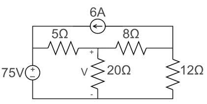
- A. 50 V
- B. 36 V
- C. 38 V
- D. 12 V
Answer: C. 38 V
Explanation: Let the bottom wire be the reference ground (0V). The node above...
Question 35
Topic: Engineering Mathematics
Solution of the below PDE
$\frac{\partial u}{\partial t}=4\frac{\partial^{2}u}{\partial x^{2}}$
$u(0,t)=u(\pi,t)=0$,
$u(x,0)=\sin(3x)$
- A. $u(x,t)=e^{-36t}\sin(3x)$
- B. $u(x,t)=-e^{-36t}\sin(3x)$
- C. $u(x,t)=-e^{9t}\sin(3x)$
- D. $u(x,t)=e^{-9t}\sin(3x)$
Answer: A. $u(x,t)=e^{-36t}\sin(3x)$
Explanation: This is a standard 1D heat equation $\frac{\partial u}{\partial t} = \alpha \frac{\partial^2 u}{\partial x^2}$ with $\alpha = 4$. The general solution satisfying the boundary conditions $u(0,t)=u(\pi,t)=0$ is $u(x,t) = \sum B_n e^{-\alpha n^2 t} \sin(nx)$.
Applying the initial condition $u(x,0) = \sin(3x)$, we can see that only the term with $n = 3$ is non-zero, and its coefficient $B_3 = 1$.
Substituting $n=3$ and $\alpha=4$ into the exponential term yields $e^{-4(3)^2 t} = e^{-36t}$.
Thus, the solution is $u(x,t) = e^{-36t}\sin(3x)$.
Question 36
Topic: Control Systems
The general form of a Lead compensator or Lag compensator in Laplace domain is :
- A. $K(1+sT_{1})(1+sT_{2})$
- B. $K(1+(1/sT_{1}))(1+sT_{2})$
- C. $K(1+sT_{1})/(1+sT_{2})$
- D. $K(1+sT_{2})/(1+(1/sT_{1}))$
Answer: C. $K(1+sT_{1})/(1+sT_{2})$
Explanation: The standard transfer function for both phase-lead and phase-lag compensators is expressed as $G_c(s) = K \frac{1 + sT_1}{1 + sT_2}$. If $T_1 > T_2$, it acts as a lead compensator, and if $T_1 < T_2$, it acts as a lag compensator.
Question 37
Topic: Network Theory
The voltage V in the circuit given below is :
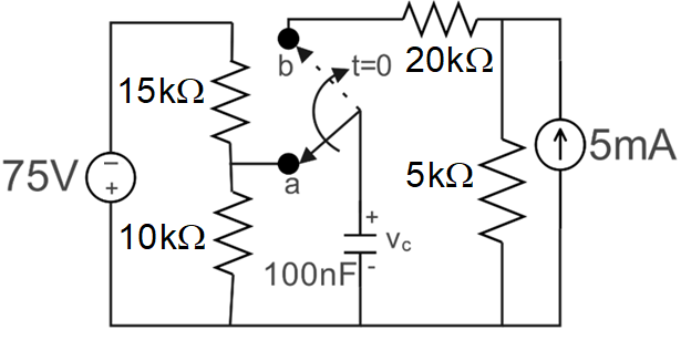
- A. 30 V, 125 V, 25 ms
- B. 30 V, 25 V, 25 ms
- C. -30 V, 125 V, 2.5 ms
- D. -30 V, 25 V, 2.5 ms
Answer: D. -30 V, 25 V, 2.5 ms
Explanation: For $t < 0$, the switch is at 'a'. The capacitor is fully charged (open circuit). The voltage across it is determined by the voltage divider of the -75V source (note the polarity: minus on top, plus on bottom) across the 15k$\Omega$ and 10k$\Omega$ resistors. $v_c(0) = -75 \times \frac{10k}{15k + 10k} = -30V$.
For $t > 0$, the switch moves to 'b'. The capacitor is now connected to a 5mA upward current source in parallel with a 5k$\Omega$ resistor, which are in series with a 20k$\Omega$ resistor.
The final voltage $v_c(\infty)$ is the Thevenin voltage of this active network. $V_{th} = 5mA \times 5k\Omega = +25V$.
The time constant $\tau = R_{eq}C$. $R_{eq}$ seen by the capacitor is $20k\Omega + 5k\Omega = 25k\Omega$. $\tau = 25k\Omega \times 100nF = 2.5$ ms.
Question 38
Topic: Analog Circuits
In a common source amplifier using an NMOS transistor, what is the impact of increasing the channel length modulation parameter ($\lambda$)?
- A. Output resistance increases
- B. Gain increases
- C. Output resistance decreases
- D. There is no change in output characteristics
Answer: C. Output resistance decreases
Explanation: The output resistance of a MOSFET is inversely proportional to the channel length modulation parameter, given by $r_0 = \frac{1}{\lambda I_D}$. Therefore, increasing the channel length modulation parameter $\lambda$ will decrease the output resistance $r_0$, which in turn reduces the overall voltage gain of the amplifier.
Question 39
Topic: Power Electronics
A single-phase inverter using bipolar PWM produces an output voltage waveform with a switching frequency much higher than the fundamental frequency. If the modulation index Ma is increased from 0.8 to 1.2, how does the amplitude of the fundamental output voltage change?
- A. It increases linearly with Ma even beyond 1
- B. It increases with Ma even beyond 1 and then saturates
- C. It saturates and remains constant beyond $Ma=1$
- D. It decreases beyond $Ma=1$
Answer: B. It increases with Ma even beyond 1 and then saturates
Explanation: In sinusoidal PWM, when the amplitude modulation index $M_a \le 1$ (linear region), the fundamental output voltage amplitude is linearly proportional to $M_a$. When $M_a$ is increased beyond 1 (overmodulation, e.g., to 1.2), the output voltage continues to increase but non-linearly. It eventually saturates to the fundamental amplitude of a pure square wave ($\frac{4}{\pi} V_d$) as $M_a$ becomes very large.
Question 40
Topic: Digital Circuits
A Mealy system produces a '1' output if the input has been 'O' for at least two consecutive clocks followed immediately by two or more consecutive '1's. The minimum number of states for this system is
Answer: C. 4
Explanation: Let's define the minimum states required to track this sequence:
S0: Initial state (or consecutive 1s not meeting the condition). If 0, go to S1.
S1: One '0' seen. If 0, go to S2. If 1, return to S0.
S2: Two or more '0's seen. If 0, stay in S2. If 1, condition met partially, go to S3 and output 0.
S3: Two or more '0's followed by one '1' seen. If 1, output 1 and stay in S3 (since the condition 'two or more consecutive 1s' remains satisfied as long as 1s continue). If 0, the sequence breaks, go to S1 and output 0.
Because S3 correctly loops on itself for continuous 1s and outputs 1, the entire machine only requires these 4 states.
Question 41
Topic: Digital Circuits
Which of the following conditions reduces the Mean Time Between Failures (MTBF) due to metastability?
- A. Decreasing flip-flop setup time
- B. Increasing metastability resolution time
- C. Increasing clock frequency and data arrival rate
- D. All of the above
Answer: C. Increasing clock frequency and data arrival rate
Explanation: The Mean Time Between Failures (MTBF) due to metastability is given by $MTBF = \frac{e^{t_r / \tau}}{T_0 f_c f_d}$, where $t_r$ is the available resolution time, $f_c$ is the clock frequency, and $f_d$ is the data toggle frequency. Increasing the clock frequency and data arrival rate increases the denominator, thereby reducing the MTBF (meaning failures happen more frequently, which degrades reliability).
Question 42
Topic: Signals and Systems
Let $x(t)=rect(t/2)$, where $rect(t/2)$ is the rectangular pulse of width 2 centered at $t=0$, i.e., $x(t)=1$ for $|t|\le1$ and 0 otherwise. What is the Fourier Transform $X(w)$ of $x(t)$?
- A. $X(w)=2~sinc(w)$
- B. $X(w)=sinc(w)$
- C. $X(w)=2~sinc(w/2)$
- D. $X(w)=sinc(w/2)$
Answer: A. $X(w)=2~sinc(w)$
Explanation: The Fourier transform of a rectangular pulse of width $T$ centered at the origin is $X(\omega) = \int_{-T/2}^{T/2} 1 \cdot e^{-j\omega t} dt = T \frac{\sin(\omega T / 2)}{\omega T / 2}$.
Here, the width $T = 2$. Substituting $T = 2$ gives $X(\omega) = 2 \frac{\sin(\omega)}{\omega}$.
Using the standard unnormalized sinc function definition $sinc(x) = \frac{\sin(x)}{x}$, this is exactly $2~sinc(\omega)$.
Question 43
Topic: Analog Circuits
The voltage V in the circuit given below is :
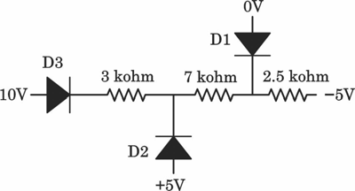
- A. D1-FB, D2-FB, D3-FB
- B. D1-FB, D2-RB, D3-FB
- C. D1-FB, D2-FB, D3-RB
- D. D1-FB, D2-RB, D3-RB
Answer: B. D1-FB, D2-RB, D3-FB
Explanation: Assume D3 and D1 are Forward Biased (ON) and D2 is Reverse Biased (OFF).
If D3 is ON, the voltage at the node left of the 3k$\Omega$ resistor is 10V.
If D1 is ON, the node between the 7k$\Omega$ and 2.5k$\Omega$ resistors ($V_B$) is clamped to 0V.
The current leaving $V_B$ through the 2.5k$\Omega$ resistor to -5V is $I_{out} = \frac{0 - (-5)}{2.5k} = 2$ mA.
The current entering $V_B$ from the left side is $I_{in} = \frac{10 - 0}{3k + 7k} = 1$ mA.
Since $I_{out} > I_{in}$, D1 must supply the remaining 1 mA current, confirming D1 is ON.
The voltage at the middle node ($V_A$, where D2 connects) is calculated via the resistor drop: $V_A = 10V - (1mA \times 3k\Omega) = 7V$.
The anode of D2 is at +5V and its cathode is at $V_A = 7V$, making it Reverse Biased. Thus, the assumption holds: D1 is FB, D2 is RB, D3 is FB.
Question 44
Topic: Control Systems
Frequency response of a system is given in the following table:
Frequency | Gain | Phase
1 | 8 | -50
10 | 1 | -155
100 | 0.25 | -180
1000 | 0.1 | -235
The Phase margin and Gain margin respectively are
- A. 4, 25
- B. 25, 4
- C. 25, 0.25
- D. 0.25, 25
Answer: B. 25, 4
Explanation: Phase Margin (PM) is evaluated at the gain crossover frequency where the magnitude is 1. From the table, at $\omega = 10$ rad/s, Gain = 1 and Phase = $-155^{\circ}$. $PM = 180^{\circ} + \angle G(j\omega) = 180^{\circ} + (-155^{\circ}) = 25^{\circ}$.
Gain Margin (GM) is evaluated at the phase crossover frequency where the phase is $-180^{\circ}$. At $\omega = 100$ rad/s, Phase = $-180^{\circ}$ and Gain = $0.25$. GM in absolute magnitude is $\frac{1}{Gain} = \frac{1}{0.25} = 4$.
Thus, Phase Margin = $25^{\circ}$ and Gain Margin = 4.
Question 45
Topic: Network Theory
The driving-point impedance of a network is given by: $Z(s)=\frac{s^{2}+3s+2}{s(s+2)}$
Which of the following statements is correct regarding the synthesis of this network?
- A. The function is not realizable using passive elements only
- B. The function can be realized using L and C elements only
- C. The function can be realized using passive elements only
- D. The function is not positive real and cannot be synthesized
Answer: C. The function can be realized using passive elements only
Explanation: Simplifying the given impedance function: $Z(s) = \frac{(s+1)(s+2)}{s(s+2)}$. Canceling the $(s+2)$ term gives $Z(s) = \frac{s+1}{s} = 1 + \frac{1}{s}$.
This corresponds precisely to a $1~\Omega$ resistor in series with a $1$ F capacitor. Since both are passive elements, the function is positive real and can be synthesized using passive elements only.
Question 46
Topic: Analog Circuits
The voltage V in the circuit given below is :
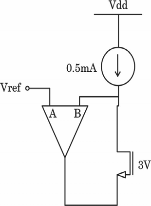
- A. Terminal A is positive. Terminal B is negative
- B. Terminal A is negative. Terminal B is positive
- C. Both of above
- D. None of the above
Answer: B. Terminal A is negative. Terminal B is positive
Explanation: 1. **Feedback Polarity:** The OPAMP drives the gate of the NMOS transistor. The drain of the NMOS is connected to terminal B. If the voltage at B increases, the OPAMP output should increase the gate voltage to turn the NMOS ON harder, pulling the drain voltage (B) back down. This requires terminal B to be the non-inverting (+) terminal. Therefore, terminal A must be the inverting (-) terminal.
2. **Gate Potential:** By virtual short, $V_B = V_{ref} = 3V$. The transistor is in saturation since it's driven by a 0.5mA current source. $I_D = \frac{1}{2} \mu_n C_{ox} (\frac{W}{L}) (V_{GS} - V_T)^2$. Substituting the values: $0.5 = \frac{1}{2} (1) (V_G - 3 - 0.7)^2$. Solving this: $1 = (V_G - 3.7)^2 \implies V_G = 3.7 + 1 = 4.7V$.
Question 47
Topic: Control Systems / Network Theory
The voltage V in the circuit given below is :
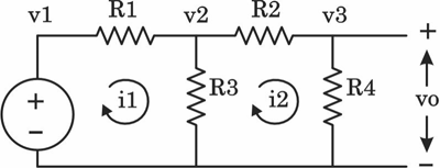
- A. Image showing SFG with correct branches
- B. Image showing SFG with incorrect branches
- C. Image showing SFG with incorrect branches
- D. Image showing SFG with incorrect branches
Answer: A. Image showing SFG with correct branches
Explanation: Writing the equations for the given circuit:
1. $i_1 = \frac{v_1 - v_2}{R_1} \implies i_1 = \frac{1}{R_1}v_1 + (-\frac{1}{R_1})v_2$
2. By KCL at node 2, current into $R_3$ is $(i_1 - i_2)$. Thus, $v_2 = (i_1 - i_2)R_3 = R_3 i_1 + (-R_3) i_2$
3. $i_2 = \frac{v_2 - v_3}{R_2} \implies i_2 = \frac{1}{R_2}v_2 + (-\frac{1}{R_2})v_3$
4. $v_3 = i_2 R_4$
These equations directly map to the signal flow graph in option (a).
Question 48
Topic: Electromagnetics / Antennas
The radiation resistance of an antenna is 63 ohms and the loss resistance is 7 ohms. If antenna has power gain of 16, then directivity is
- A. 48.26 dB
- B. 12.5 dB
- C. 17.77 dB
- D. 24.7 dB
Answer: B. 12.5 dB
Explanation: Radiation efficiency $e = \frac{R_{rad}}{R_{rad} + R_{loss}} = \frac{63}{63 + 7} = \frac{63}{70} = 0.9$.
The relationship between Gain ($G$) and Directivity ($D$) is $G = e \times D$.
$16 = 0.9 \times D \implies D = \frac{16}{0.9} = 17.77$ (linear scale).
Converting Directivity to dB: $D_{dB} = 10 \log_{10}(17.77) \approx 12.5$ dB.
Question 49
Topic: Digital Circuits
The voltage V in the circuit given below is :
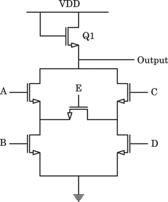
- A. $Y=(AB+CD+CEB)$
- B. $Y=(AB+CD+AED+CEB)$
- C. $Y=(AB+AED+CEB)$
- D. $Y=(AB+CD)$
Answer: B. $Y=(AB+CD+AED+CEB)$
Explanation: The given circuit consists of an NMOS pull-down network configured as a bridge (A, B, C, D, and cross-connecting transistor E). The output is pulled low when there is a conducting path to ground. The four possible paths to ground are through transistors:
1. A and B ($AB$)
2. C and D ($CD$)
3. A, E, and D ($AED$)
4. C, E, and B ($CEB$)
Therefore, the logic function evaluating the ON condition of the pull-down network is $Y = AB + CD + AED + CEB$.
Question 50
Topic: Control Systems
Consider the following statements:
A proportional plus derivative controller
(i) Has high sensitivity
(ii) Improves the steady state accuracy
(iii) Increases the stability of the system
Which of the following statements are correct?
- A. (i), (ii) and (iii)
- B. (i) and (ii)
- C. (ii) and (iii)
- D. (i) and (iii)
Answer: D. (i) and (iii)
Explanation: A Proportional-Derivative (PD) controller improves the transient response by adding phase lead, thereby increasing the system's stability margin (iii is true). Because the derivative action amplifies high-frequency noise, it makes the system highly sensitive to noise (i is true). However, a PD controller does not improve steady-state accuracy; that requires an integral (I) controller. Therefore, (ii) is false.
Question 51
Topic: Electromagnetics
A boundary separates two magnetic materials of permeability $\mu_{1}$ and $\mu_{2}$. The magnetic field vector in $\mu_{1}$ is $H_{1}$ with a normal component $H_{n_{1}}$ and tangential component $H_{t_{1}}$ while that in $\mu_{2}$ is $H_{2}$ with a normal component $H_{n_{2}}$ and tangential component $H_{t_{2}}$ Then the derived condition would be
- A. $H_{1}=H_{2}$ and $H_{t_{1}}=H_{t_{2}}$
- B. $H_{t_{1}}=H_{t_{2}}$ and $\mu_{1}H_{n_{1}}=\mu_{2}H_{n_{2}}$
- C. $H_{1}=H_{2}$ and $\mu_{1}H_{n_{1}}=\mu_{2}H_{n_{2}}$
- D. $H_{1}=H_{2}$, $H_{t_{1}}=H_{t_{2}}$ and $\mu_{1}H_{n_{1}}=\mu_{2}H_{n_{2}}$
Answer: B. $H_{t_{1}}=H_{t_{2}}$ and $\mu_{1}H_{n_{1}}=\mu_{2}H_{n_{2}}$
Explanation: At the boundary between two magnetic media, assuming no surface current density, the tangential component of the magnetic field intensity ($H$) is continuous: $H_{t_1} = H_{t_2}$. The normal component of the magnetic flux density ($B$) is always continuous: $B_{n_1} = B_{n_2}$. Since $B = \mu H$, this gives $\mu_1 H_{n_1} = \mu_2 H_{n_2}$.
Question 52
Topic: Analog Circuits
The voltage V in the circuit given below is :
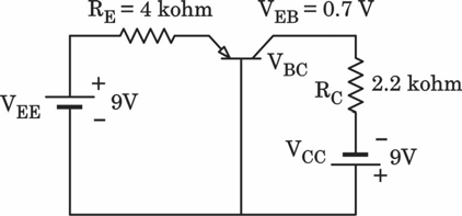
- A. 7.47 V
- B. 8.43 V
- C. 4.47 V
- D. 0.47 V
Answer: C. 4.47 V
Explanation: The base is grounded ($V_B = 0V$). The emitter is forward-biased, so $V_E = -0.7V$.
The emitter current is $I_E = \frac{V_E - (-V_{EE})}{R_E} = \frac{-0.7 - (-9)}{4k\Omega} = \frac{8.3}{4} = 2.075$ mA.
The collector current is $I_C = \alpha I_E = 0.992 \times 2.075 = 2.0584$ mA.
The collector voltage is $V_C = V_{CC} - I_C R_C = 9 - (2.0584 \times 2.2) = 9 - 4.528 = 4.472$ V.
The magnitude of the base-collector voltage is $|V_{BC}| = |V_B - V_C| = |0 - 4.472| = 4.47$ V.
Question 53
Topic: Control Systems
The voltage V in the circuit given below is :
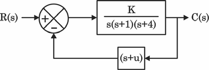
- A. $\frac{u-1}{u}$
- B. $\frac{u-1}{u^{2}}$
- C. $\frac{u^{2}}{u-1}$
- D. $\frac{1}{u-1}$
Answer: D. $\frac{1}{u-1}$
Explanation: The closed-loop transfer function is $\frac{C(s)}{R(s)} = \frac{G(s)}{1+G(s)H(s)} = \frac{K}{s(s+1)(s+4) + K(s+u)}$.
For a unit step input $R(s) = \frac{1}{s}$, the steady-state output is $c(\infty) = \lim_{s \to 0} s C(s) = \lim_{s \to 0} \frac{K}{s(s+1)(s+4) + K(s+u)} = \frac{K}{Ku} = \frac{1}{u}$.
The steady-state error is $e_{ss} = 1 - c(\infty) = 1 - \frac{1}{u} = \frac{u-1}{u}$.
The sensitivity of $e_{ss}$ with respect to $u$ is $S_u^{e_{ss}} = \frac{u}{e_{ss}} \frac{\partial e_{ss}}{\partial u}$.
$\frac{\partial e_{ss}}{\partial u} = \frac{\partial}{\partial u} (1 - u^{-1}) = \frac{1}{u^2}$.
$S_u^{e_{ss}} = \frac{u}{(u-1)/u} \times \frac{1}{u^2} = \frac{u^2}{u-1} \times \frac{1}{u^2} = \frac{1}{u-1}$.
Question 54
Topic: Electromagnetics
Consider a lossy dielectric with complex permittivity $\epsilon=\epsilon^{\prime}-j\epsilon^{\prime\prime}$. The loss tangent is defined as $\tan~\delta=\epsilon^{\prime\prime}/\epsilon^{\prime}$. What does $\tan~\delta\rightarrow\infty$ physically imply?
- A. The medium behaves like a perfect conductor
- B. The medium behaves like a lossless dielectric
- C. The medium behaves like a perfect insulator
- D. The displacement current dominates conduction current
Answer: A. The medium behaves like a perfect conductor
Explanation: The loss tangent $\tan \delta = \frac{\sigma}{\omega \epsilon'} = \frac{\epsilon''}{\epsilon'}$. It represents the ratio of the conduction current density to the displacement current density. As $\tan \delta \to \infty$, the conduction current heavily dominates over the displacement current, which is the defining characteristic of a good conductor. Thus, the medium behaves like a perfect conductor.
Question 55
Topic: Analog Circuits
The voltage V in the circuit given below is :
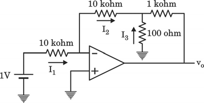
- A. $I_{1}=100~\mu A$, $I_{2}=100~\mu A$, $I_{3}=10~mA$
- B. $I_{1}=10~mA$, $I_{2}=1~\mu A$, $I_{3}=100~\mu A$
- C. $I_{1}=50~\mu A$, $I_{2}=100~\mu A$, $I_{3}=100~\mu A$
- D. $I_{1}=100~mA$, $I_{2}=1~\mu A$, $I_{3}=100~\mu A$
Answer: A. $I_{1}=100~\mu A$, $I_{2}=100~\mu A$, $I_{3}=10~mA$
Explanation: The non-inverting terminal is grounded, so by virtual short concept, the inverting terminal $V_- = 0V$.
$I_1$ flows from the 1V source to $V_-$. $I_1 = \frac{1V - 0V}{10 k\Omega} = 100 \mu A$.
Since the OPAMP input current is zero, $I_2$ must equal $I_1$. Thus, $I_2 = 100 \mu A$.
The voltage at the intermediate node $V_x$ is $V_- - I_2(10 k\Omega) = 0 - (100\mu A \times 10 k\Omega) = -1V$.
$I_3$ flows upward from ground (0V) to $V_x$. $I_3 = \frac{0V - (-1V)}{100 \Omega} = \frac{1V}{100 \Omega} = 10 mA$.
Question 56
Topic: Control Systems
The voltage V in the circuit given below is :
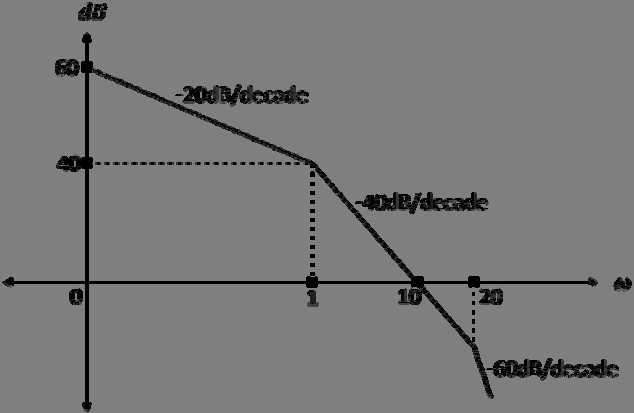
- A. $\frac{2000}{s(s-1)(s+20)}$
- B. $\frac{2000}{s(s-1)(s-20)}$
- C. $\frac{1000}{s(s+1)(s-20)}$
- D. $\frac{2000}{s(s+1)(s+20)}$
Answer: D. $\frac{2000}{s(s+1)(s+20)}$
Explanation: The initial slope is -20 dB/dec, indicating a pole at the origin ($1/s$).
At $\omega=1$, the slope changes from -20 dB/dec to -40 dB/dec, meaning there is a simple pole at $s=1$.
At $\omega=20$, the slope changes from -40 dB/dec to -60 dB/dec, meaning another simple pole at $s=20$.
The general form is $H(s) = \frac{K_0}{s(s/1 + 1)(s/20 + 1)}$.
At $\omega=1$, the magnitude of the $K_0/s$ term dictates the graph before corner frequencies. So $20 \log_{10}(K_0 / 1) = 40$ dB $\implies K_0 = 100$.
$H(s) = \frac{100}{s(s+1)(s/20 + 1)} = \frac{2000}{s(s+1)(s+20)}$.
Question 57
Topic: Digital Communications
A communication channel has a bandwidth of 3 kHz and Signal-to-Noise Ratio (SNR) of 30 dB. What is the channel capacity?
- A. ~30 kbps
- B. ~20 kbps
- C. ~2.1 kbps
- D. ~3.3 kbps
Answer: A. ~30 kbps
Explanation: First, convert the SNR from dB to linear scale: $SNR_{linear} = 10^{30/10} = 10^3 = 1000$.
Using Shannon's Channel Capacity theorem: $C = B \log_2(1 + SNR)$.
$C = 3000 \times \log_2(1 + 1000) = 3000 \times \log_2(1001)$.
Since $\log_2(1024) = 10$, $\log_2(1001)$ is approximately 9.967.
$C \approx 3000 \times 9.967 = 29901$ bps, which is roughly 30 kbps.
Question 58
Topic: Analog Circuits
The voltage V in the circuit given below is :
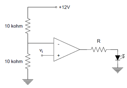
- A. Less than 6 V
- B. More than 6 V
- C. Less than 12 V
- D. More than 12 V
Answer: B. More than 6 V
Explanation: The OPAMP operates as a comparator. The voltage at the inverting terminal $V_-$ is fixed by the voltage divider: $V_- = 12V \times \frac{10 k\Omega}{10 k\Omega + 10 k\Omega} = 6V$.
The non-inverting terminal $V_+$ is connected to $V_i$.
For the LED to turn ON, the output of the OPAMP must be positive, which requires $V_+ > V_-$.
Therefore, the LED will be ON when $V_i > 6V$.
Question 59
Topic: Analog Circuits
The voltage V in the circuit given below is :
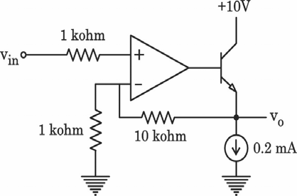
- A. Series-Series
- B. Shunt-Series
- C. Series-Shunt
- D. Shunt-Shunt
Answer: C. Series-Shunt
Explanation: The feedback network senses the output voltage $V_o$ (taken from the emitter node in parallel/shunt) and feeds a proportion of it back to the inverting terminal of the OPAMP. Since the input signal is applied to the non-inverting terminal, the feedback effectively subtracts from the input in series (mixing voltages in the input loop). Therefore, this topology represents a Series-Shunt (voltage-series) feedback amplifier.
Question 60
Topic: Signals and Systems
What is the Nyquist rate for a continuous time signal $x(t)=5~\cos(100\pi t)+2~\sin(200\pi t)$?
- A. 100 Hz
- B. 200 Hz
- C. 400 Hz
- D. 50 Hz
Answer: B. 200 Hz
Explanation: The signal contains two frequency components:
1. $\omega_1 = 100\pi \implies f_1 = 50$ Hz.
2. $\omega_2 = 200\pi \implies f_2 = 100$ Hz.
The maximum frequency component present in the signal is $f_{max} = 100$ Hz.
The Nyquist rate is defined as twice the maximum frequency: $f_s = 2 \times f_{max} = 2 \times 100 = 200$ Hz.
Question 61
Topic: Power Electronics
In a single-phase full-wave controlled rectifier using SCRs with a resistive load, the firing angle is set to $\alpha=60^{\circ}.$ Which of the following statements is TRUE regarding the average output voltage (V_avg)? Assume ideal conditions. $V_{m}=$ the peak input voltage
- A. $V_{\_}avg=(V_{m}/\pi)(1+\cos(60^{\circ}))$
- B. $V_{\_}avg=(2V_{m}/\pi)(1-\cos(60^{\circ}))$
- C. $V_{\_}avg=(2V_{m}/\pi)(1+\cos(60^{\circ}))$
- D. $V_{\_}avg=V_{m}\cos(60^{\circ})$
Answer: A. $V_{\_}avg=(V_{m}/\pi)(1+\cos(60^{\circ}))$
Explanation: For a single-phase full-wave fully controlled rectifier with a purely resistive load, the average output voltage is calculated by integrating the output waveform over one half-cycle: $V_{avg} = \frac{1}{\pi} \int_{\alpha}^{\pi} V_m \sin(\omega t) d(\omega t)$. Evaluating the integral gives $V_{avg} = \frac{V_m}{\pi} [-\cos(\omega t)]_{\alpha}^{\pi} = \frac{V_m}{\pi} (1 + \cos\alpha)$. Substituting $\alpha = 60^{\circ}$ yields $V_{avg} = (V_m/\pi)(1+\cos(60^{\circ}))$.
Question 62
Topic: Digital Communications
The eye diagram of a digital communication system closes vertically and horizontally due to
- A. Inter-symbol interference only
- B. Timing jitter and ISI
- C. AWGN only
- D. Synchronization drift only
Answer: B. Timing jitter and ISI
Explanation: In an eye diagram, the vertical opening indicates the system's immunity to noise and is reduced primarily by Inter-Symbol Interference (ISI) and additive noise. The horizontal opening represents the time interval over which the signal can be reliably sampled and is reduced by timing jitter and phase variations. Therefore, the diagram closes both vertically and horizontally due to the combined effects of Timing jitter and ISI.
Question 63
Topic: Electronic Measurements and Instrumentation
A strain gauge with a gauge factor of 2.0 is connected in a Wheatstone bridge and subjected to a strain of 250 \mu\epsilon. What is the relative change in resistance (AR/R) of the gauge?
- A. 250 ppm
- B. 125 ppm
- C. 500 ppm
- D. 1000 ppm
Answer: C. 500 ppm
Explanation: The Gauge Factor (GF) is defined as the ratio of relative change in resistance to the mechanical strain: $GF = \frac{\Delta R / R}{\epsilon}$.
Rearranging gives $\frac{\Delta R}{R} = GF \times \epsilon$.
Substituting the given values: $\frac{\Delta R}{R} = 2.0 \times 250 \times 10^{-6} = 500 \times 10^{-6}$.
In parts per million (ppm), $500 \times 10^{-6}$ is equal to 500 ppm.
Question 64
Topic: Electronic Devices and Circuits
Which of the following conditions will maximize the diffusion current in a semiconductor?
- A. Uniform doping profile
- B. High electric field
- C. Steep concentration gradient
- D. Zero temperature gradient
Answer: C. Steep concentration gradient
Explanation: Diffusion current in a semiconductor occurs due to the random thermal motion of charge carriers from a region of high concentration to a region of low concentration. It is governed by Fick's first law, making it directly proportional to the concentration gradient (e.g., $J_p = -q D_p \frac{dp}{dx}$). Therefore, a steep (large) concentration gradient will maximize the diffusion current.
Question 65
Topic: Network Theory
In an AC circuit, a resistor of $10~\Omega$ is in series with an inductor of reactance $10~\Omega$. What is the power factor of the circuit?
- A. 0.5 lagging
- B. 0.707 lagging
- C. 1.0 (unity)
- D. 0.866 leading
Answer: B. 0.707 lagging
Explanation: The impedance of the series RL circuit is $Z = R + jX_L = 10 + j10~\Omega$.
The magnitude of impedance is $|Z| = \sqrt{R^2 + X_L^2} = \sqrt{10^2 + 10^2} = 10\sqrt{2}~\Omega$.
The power factor is $\cos \phi = \frac{R}{|Z|} = \frac{10}{10\sqrt{2}} = \frac{1}{\sqrt{2}} \approx 0.707$.
Since the circuit is inductive, the current lags the voltage, so the power factor is 0.707 lagging.
Question 66
Topic: Digital Circuits
In a CMOS inverter operating in the transition region, what best describes the operation of NMOS and PMOS transistors?
- A. Both are in cutoff region
- B. Only PMOS conducts
- C. Both are conducting
- D. Only NMOS conducts
Answer: C. Both are conducting
Explanation: During the transition region of a CMOS inverter (when the input voltage is approximately around $V_{DD}/2$), the input voltage is higher than the threshold voltage of the NMOS transistor and lower than $V_{DD} - |V_{tp}|$, which means both transistors are simultaneously turned ON and conducting. This leads to a momentary short-circuit (crowbar) current flowing directly from $V_{DD}$ to ground.
Question 67
Topic: Electronic Measurements and Instrumentation
An LVDT (Linear Variable Differential Transformer) has a sensitivity of 2 mV/mm/V (output per mm of displacement per volt of excitation). If it is excited with 5 V AC and produces an output of 30 mV, what is the core displacement?
- A. 1 mm
- B. 2 mm
- C. 3 mm
- D. None of the above
Answer: C. 3 mm
Explanation: The output voltage of an LVDT is given by $V_{out} = \text{Sensitivity} \times \text{Displacement} \times V_{in}$.
Rearranging for displacement: $\text{Displacement} = \frac{V_{out}}{\text{Sensitivity} \times V_{in}}$.
Substitute the given values: $\text{Displacement} = \frac{30~\text{mV}}{2~\text{mV/mm/V} \times 5~\text{V}} = \frac{30}{10} = 3$ mm.
Question 68
Topic: Electronic Devices and Circuits
In an N-type semiconductor, the Fermi level $E_F$ equals:
- A. $E_C - kT \ln(N_C/N_D)$
- B. $E_C - kT \ln(N_D/N_C)$
- C. $E_V + kT \ln(N_C/N_D)$
- D. $E_V - kT \ln(N_C/N_D)$
Answer: A. $E_C - kT \ln(N_C/N_D)$
Explanation: In an n-type semiconductor at thermal equilibrium, assuming complete ionization of donor atoms, the electron concentration in the conduction band is approximately equal to the donor concentration, $n \approx N_D$.
The carrier concentration is also given by $n = N_C e^{-(E_C - E_F)/(kT)}$.
Equating the two: $N_D = N_C e^{-(E_C - E_F)/(kT)}$.
Taking the natural logarithm of both sides: $\ln(N_D/N_C) = -(E_C - E_F)/(kT) \implies E_C - E_F = -kT \ln(N_D/N_C) = kT \ln(N_C/N_D)$.
Thus, $E_F = E_C - kT \ln(N_C/N_D)$.
Question 69
Topic: Power Electronics
In a single-phase full-bridge inverter with square wave output, what is the amplitude of the third harmonic component if the fundamental amplitude is V?
- A. $V/3$
- B. $V/5$
- C. $V/9$
- D. $V/7$
Answer: A. $V/3$
Explanation: The Fourier series for a square wave output voltage of a single-phase full-bridge inverter is given by $v_o(t) = \sum_{n=1,3,5,...}^{\infty} \frac{4V_{dc}}{n\pi} \sin(n\omega t)$.
The amplitude of the $n^{th}$ harmonic is $V_n = \frac{4V_{dc}}{n\pi}$.
The fundamental amplitude ($n=1$) is $V_1 = \frac{4V_{dc}}{\pi} = V$.
For the third harmonic ($n=3$), the amplitude is $V_3 = \frac{4V_{dc}}{3\pi} = \frac{1}{3} \left(\frac{4V_{dc}}{\pi}\right) = \frac{V}{3}$.
Question 70
Topic: Electronic Devices and Circuits
Select the value closest to the forbidden band in Germanium at 0K:
- A. 0.78 eV
- B. 1.00 eV
- C. 0.01 eV
- D. 1.21 eV
Answer: A. 0.78 eV
Explanation: The forbidden energy band gap of a semiconductor depends on temperature. For Germanium (Ge), the band gap energy is approximately 0.67 eV at room temperature (300K) and widens as temperature decreases, reaching about 0.78 eV at absolute zero (0K). By contrast, Silicon is approximately 1.21 eV at 0K.
Question 71
Topic: Signals and Systems
If a discrete-time LTI system has a frequency response $H(e^{j\omega})=1/(1-0.5e^{-j\omega})$, what is its impulse response $h[n]$?
- A. $(0.5)^{n}u[n]$
- B. $(0.5)^{(n-1)}u[n-1]$
- C. $u[n]-0.5u[n-1]$
- D. $\delta[n]-0.5\delta[n-1]$
Answer: A. $(0.5)^{n}u[n]$
Explanation: The given frequency response $H(e^{j\omega})$ represents the Discrete-Time Fourier Transform (DTFT) of the impulse response $h[n]$. The general DTFT pair for a right-sided exponential sequence is $\mathcal{F}\\{a^n u[n]\\} = \frac{1}{1 - a e^{-j\omega}}$, provided $|a| < 1$. Matching this with the given $H(e^{j\omega})$, we have $a = 0.5$. Therefore, the inverse DTFT gives the impulse response $h[n] = (0.5)^n u[n]$.
Question 72
Topic: Electronic Devices and Circuits
Pinch-off voltage in an FET is:
- A. The gate-to-source voltage that gives zero drain current
- B. The drain voltage that gives zero drain current
- C. The gate source voltage that gives unity drain current
- D. The drain voltage that gives infinite drain current
Answer: A. The gate-to-source voltage that gives zero drain current
Explanation: The pinch-off voltage ($V_p$ or $V_{GS(off)}$) in a Field Effect Transistor (FET), particularly a JFET, is defined as the reverse-bias gate-to-source voltage at which the depletion regions from opposite sides of the channel completely merge, cutting off the conductive path. This effectively reduces the drain current to zero.
Question 73
Topic: Control Systems
Consider the system with transfer function $H(s)=(s+1)/(s^{2}+2s+2)$. Which of the following best describes the nature of its poles?
- A. Real and equal
- B. Real and distinct
- C. Complex conjugates with negative real parts
- D. Purely imaginary
Answer: C. Complex conjugates with negative real parts
Explanation: The poles of a transfer function are found by setting the denominator polynomial to zero: $s^2 + 2s + 2 = 0$.
Using the quadratic formula to solve for $s$: $s = \frac{-2 \pm \sqrt{2^2 - 4(1)(2)}}{2} = \frac{-2 \pm \sqrt{4 - 8}}{2} = \frac{-2 \pm \sqrt{-4}}{2} = \frac{-2 \pm j2}{2} = -1 \pm j1$.
These roots are a complex conjugate pair with a negative real part (-1), meaning the system is underdamped and stable.
Question 74
Topic: Digital Circuits / Analog Circuits
The output of a Schmitt trigger depends on:
- A. Only input value
- B. Clock transitions
- C. Hysteresis in threshold voltages
- D. Fan-in of the gate
Answer: C. Hysteresis in threshold voltages
Explanation: A Schmitt trigger is a comparator circuit with positive feedback that introduces two different threshold voltage levels (an upper trigger point and a lower trigger point). This difference is called hysteresis. Because of this hysteresis, the output state does not just depend on the instantaneous input value, but also on the previous state of the output, making it highly immune to noise.
Question 75
Topic: Signals and Systems
Which of the following systems is "not" causal?
- A. $h[n]=\delta[n]$
- B. $h[n]=u[n]$
- C. $h[n]=\delta[n]+\delta[n+1]$
- D. $h[n]=(0.5)^{n}u[n]$
Answer: C. $h[n]=\delta[n]+\delta[n+1]$
Explanation: A discrete-time linear time-invariant (LTI) system is causal if and only if its impulse response $h[n] = 0$ for all $n < 0$.
Looking at option (c), $h[n] = \delta[n] + \delta[n+1]$. If we evaluate this at $n = -1$, we get $h[-1] = \delta[-1] + \delta[-1+1] = 0 + \delta[0] = 1$. Since $h[-1] \neq 0$, the system anticipates future inputs and is therefore non-causal.
Question 76
Topic: Microprocessors and Microcontrollers
Four memory chips of $4\times4$ size have their address bus connected together. This system will be of size
- A. $256\times4$
- B. $16\times4$
- C. $4\times16$
- D. $8\times4$
Answer: C. $4\times16$
Explanation: A $4\times4$ memory chip implies it has 4 addresses (words) and each address stores 4 bits. If the address buses of 4 such chips are connected in parallel, all chips are selected simultaneously by the same address. The number of addressable locations remains 4. However, their data buses are combined side-by-side to increase the word length. The new word length is $4 \text{ chips} \times 4 \text{ bits/chip} = 16 \text{ bits}$. Thus, the overall system size is $4 \times 16$.
Question 77
Topic: Electronic Measurements and Instrumentation
Which of the following voltmeters will have the least loading effect on a $100~k\Omega$ source?
- A. $10~k\Omega/V$, 10 V range
- B. $20~k\Omega/V$, 10 V range
- C. $1~M\Omega$ digital voltmeter
- D. $50~k\Omega/V$, 5 V range
Answer: C. $1~M\Omega$ digital voltmeter
Explanation: Loading effect in voltage measurement is minimized when the input resistance of the voltmeter is as high as possible.
Calculate the total internal resistance for each option:
(a) $10~k\Omega/V \times 10 V = 100~k\Omega$
(b) $20~k\Omega/V \times 10 V = 200~k\Omega$
(c) $1~M\Omega = 1000~k\Omega$
(d) $50~k\Omega/V \times 5 V = 250~k\Omega$
The $1~M\Omega$ digital voltmeter possesses the highest internal resistance, hence it draws the least current and introduces the least loading effect.
Question 78
Topic: Digital Circuits
In a 4-bit ripple counter using JK flip-flops, the maximum frequency of input clock is limited due to:
- A. Propagation delay
- B. Setup time
- C. Hold time
- D. Fan-in
Answer: A. Propagation delay
Explanation: In an asynchronous (ripple) counter, the clock input of each subsequent flip-flop is triggered by the output of the preceding one. Consequently, the propagation delay of each flip-flop accumulates. For an $n$-bit counter with flip-flop delay $t_{pd}$, the total settling time is $n imes t_{pd}$. To ensure reliable operation, the clock period $T_{clk}$ must be greater than this cumulative delay, directly limiting the maximum operating frequency ($f_{max} \le 1/(n \cdot t_{pd})$).
Question 79
Topic: Network Theory
The voltage V in the circuit given below is :
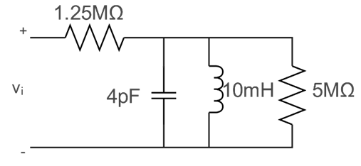
- A. 25 Mrad/s, 250 Krad/s, 100
- B. 5 Mrad/s, 250 Krad/s, 20
- C. 5 Mrad/s, 25 Krad/s, 200
- D. None of the above
Answer: B. 5 Mrad/s, 250 Krad/s, 20
Explanation: First, convert the circuit to a standard parallel RLC form by combining the resistors. The equivalent parallel resistance is $R_p = 1.25 M\Omega || 5 M\Omega = \frac{1.25 \times 5}{1.25 + 5} = 1 M\Omega$.
Given $L = 10 mH$ and $C = 4 pF$.
Resonant frequency: $\omega_o = \frac{1}{\sqrt{LC}} = \frac{1}{\sqrt{10\times 10^{-3} \times 4\times 10^{-12}}} = \frac{1}{\sqrt{40\times 10^{-15}}} = 5 \times 10^6$ rad/s = 5 Mrad/s.
Quality factor: $Q = \omega_o R_p C = (5\times 10^6) \times (1\times 10^6) \times (4\times 10^{-12}) = 20$.
Bandwidth: $\beta = \frac{\omega_o}{Q} = \frac{5\times 10^6}{20} = 0.25\times 10^6$ rad/s = 250 Krad/s.
Question 80
Topic: Network Theory
The voltage V in the circuit given below is :
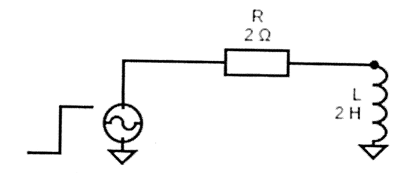
- A. 0V
- B. 1 V
- C. 2 V
- D. Infinity
Answer: B. 1 V
Explanation: A unit step input implies $V_{in}(t) = 1$ V for $t \ge 0$. Prior to $t=0$, the circuit is unenergized, so the initial current $i(0^-) = 0$. Because the current through an inductor cannot change instantaneously, the current just after the switch closes is $i(0^+) = i(0^-) = 0$ A. Applying Kirchhoff's Voltage Law (KVL) at $t = 0^+$: $V_{in}(0^+) = i(0^+) R + V_L(0^+)$. Substituting the values: $1 = (0 \times 2) + V_L(0^+)$, which results in $V_L(0^+) = 1$ V.
Question 81
Topic: General Aptitude
What was the day of the week on 28th May, 2006?
- A. Thursday
- B. Friday
- C. Saturday
- D. Sunday
Answer: D. Sunday
Question 82
Topic: General Aptitude
Fact 1 : Jessica has four children.
Fact 2 : Two of the children have blue eyes and two of the children have brown eyes.
Fact 3 : Half of the children are girls.
If the first three statements are facts, which of the following statements must also be a fact?
I. At least one girl has blue eyes.
II. Two of the children are boys.
III. The boys have brown eyes.
- A. I only
- B. II only
- C. II and III only
- D. None of the statements is a known fact
Answer: B. II only
Question 83
Topic: General Aptitude
Many business offices are located in buildings having 2-8 floors. If a building has more than 3 floors, it has a lift. If the above statements are true, which of the following must be true?
- A. 2nd floors do not have lifts
- B. 7th floors have lifts
- C. Only floors above the 3rd floors have lifts
- D. All floors may be reached by lifts
Answer: B. 7th floors have lifts
Question 84
Topic: General Aptitude
A cube has a volume of 8 cubic metres. If each side is doubled in length what will its new volume be in cubic metres?
Answer: C. 64
Question 85
Topic: General Aptitude
In a mixture of 45 litres, the ratio of sugar solution to salt solution is 1 : 2. What is the amount of sugar solution to be added if the ratio has to be 2 : 1?
- A. 15 litres
- B. 45 litres
- C. 55 litres
- D. 65 litres
Answer: B. 45 litres
Question 86
Topic: General Aptitude
Which of the following mentioned standard probability density functions is applicable to discrete Random Variables?
- A. Gaussian Distribution
- B. Poisson Distribution
- C. Rayleigh Distribution
- D. Exponential Distribution
Answer: B. Poisson Distribution
Question 87
Topic: General Aptitude
Andre and Betty together weigh 150 pounds. Betty and Chris together 180 pounds. Andre, Chris and David together weigh 360 pounds. Altogether, the four of them weigh 450 pounds. How much does David weigh?
- A. 60 Pounds
- B. 90 Pounds
- C. 160 Pounds
- D. 210 Pounds
Answer: B. 90 Pounds
Question 88
Topic: General Aptitude
Statements : Some books are tables. Some tables are mirrors.
Conclusions :
I. Some mirrors are books.
II. No book is mirror.
- A. Only conclusion II follows
- B. Only conclusion I follows
- C. Either I or II follows
- D. Both I and II follow
Answer: C. Either I or II follows
Question 89
Topic: General Aptitude
Statements : No women teacher can play. Some women teachers are athletes.
Conclusions :
I. Male athletes can play.
II. Some athletes can play (Tough).
- A. Only conclusion I follows
- B. Only conclusion II follows
- C. Either I or II follows
- D. Neither I nor II follows
Answer: B. Only conclusion II follows
Question 90
Topic: General Aptitude
Which one will replace the question mark?
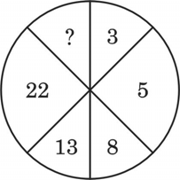
Question 91
Topic: General Aptitude
In this, you are given a combination of alphabets and/or numbers followed by four alternatives (a), (b), (c) and (d). Choose the alternative which closely resembles the mirror image of the given combination.
Question 92
Topic: General Aptitude
Observe the given figure and answer question below. If 50 play Football, 40 play Cricket and 30 play Basketball, then what is the number of players who play Football or Cricket but not Basketball?
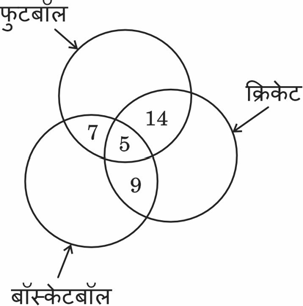
Answer: A. 45
Question 93
Topic: General Aptitude
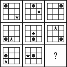
Which of the following boxes should replace the question mark (?) to complete the pattern?
Question 94
Topic: General Aptitude
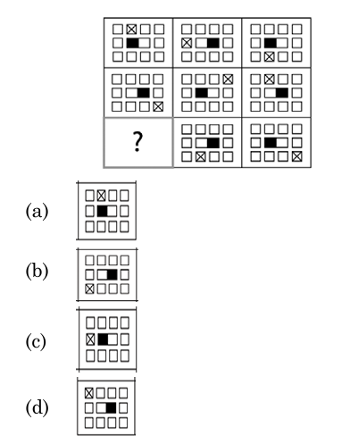
Choose which one of the options best fits the missing symbol?
Question 95
Topic: General Aptitude
Which figure completes the series?